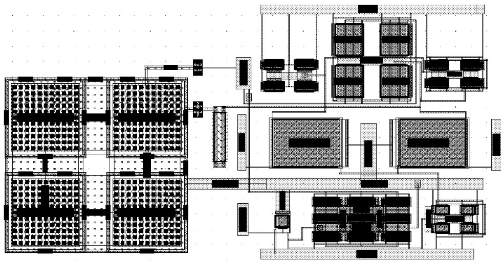
2-stage OTA Design
Designed a 2-stage Operational Transconductance Amplifier for the specified parameters and implemented it using Cadence Virtuoso

Guide: Prof. Rajesh Zele
I worked on this project as part of the course EE618: CMOS Analog VLSI Design taken by Prof. Rajesh Zele. To get us familiarized with Virtuoso, we were tasked with design the schematic and layout for a CMOS Inverter with specified rise and fall times. We were also required to perform post-layout simulations by incorporating parasitic capacitances and observing the change in the output voltage. The final project was to design and simulate a 2-stage OTA with RC compensation for the given parameters of noise, gain, slew rate, unity gain frequency, and phase margin. The final layout for the OTA had a 50dB gain, unity-gain frequency of 108MHz, 67.4 degree phase margin, all within a power budget of 0.22mW.